
Today’s electronic devices—from advanced IoT modules and industrial automation controllers to high-speed networking equipment and EV battery management systems—require compact form factors and powerful performance. This shift has dramatically increased the demand for multi-layer PCBs and high-density interconnect (HDI) structures , where reliability is not just a requirement but the foundation of product success.
For OEMs, engineering teams, and hardware developers, the challenge is ensuring that complex multilayer and HDI assemblies maintain long-term electrical stability, mechanical durability, and manufacturing consistency. Many manufacturers struggle with these technical demands because multilayer PCBs require expertise in materials, lamination, signal integrity, drilling, plating, reflow behavior, and overall turnkey workflow control.
This is where FastTurn PCB
) has earned strong global trust. Through advanced engineering processes, strict quality standards, and a vertically integrated turnkey pcba assembly workflow, FastTurn delivers highly reliable multilayer and HDI boards for a wide range of applications.
1. Advanced Lamination and Stackup Engineering for Multi-Layer Reliability
Stackup design and lamination quality are central to multilayer PCB reliability. FastTurn PCB uses engineering-driven processes to ensure structural integrity and consistent electrical performance.
Key lamination quality controls include:
Precise dielectric thickness control
Uniform resin flow during lamination
Low-void lamination conditions
Multiple-lamination-cycle management for HDI
Balanced stackups to minimize warpage
Selection of high-Tg, low-loss materials for high-speed designs
These controls reduce the risk of delamination, dielectric breakdown, and impedance inconsistency—common failure modes in multilayer PCBs.
2. High-Precision Drilling, Laser Microvias, and Via Reliability
High-density assemblies depend heavily on via reliability. FastTurn offers:
Mechanical Drilling
- Extremely accurate hole positioning
- Consistent annular ring tolerances
Laser Microvia Formation
- Controlled depth drilling
- Clean, debris-free hole walls
- Consistent diameter for stacked and staggered vias
Via Reliability Processes
- Copper plating thickness verification
- Resin plug and via-in-pad validation
- Microsection analysis
- Thermal cycling reliability testing
Because microvias and via-in-pad structures are used for modern HDI designs (such as those using BGAs or fine-pitch processors), these processes ensure long-term electrical connectivity.
3. Controlled Impedance and High-Speed Signal Integrity
OEMs working with high-speed digital or RF boards require precise impedance control.
FastTurn ensures:
- Verified impedance models
- Tight trace width and spacing tolerances
- Stable dielectric constant materials
- Consistent copper thickness
- EMC/EMI-conscious routing structures
- Testing and impedance reporting (when requested)
These controls help maintain signal integrity—critical for telecom, networking, server, storage, and EV control boards.
4. Superior Surface Finish and Material Reliability
Surface finish directly affects solder joint quality. FastTurn offers a range of finishes—including ENIG, ENEPIG, OSP, immersion silver, immersion tin—selected based on application.
ENIG/ENEPIG benefits for HDI and multilayer boards:
- Excellent flatness for BGA placement
- Strong oxidation resistance
- Stable solder joint performance
- Balanced shelf life and electrical reliability
Material reliability extends to:
- High-Tg FR-4 for thermal stability
- Low-loss materials for RF/high-speed designs
- Halogen-free materials for environmental compliance
OEMs rely on FastTurn because material selection and process control directly influence long-term durability.
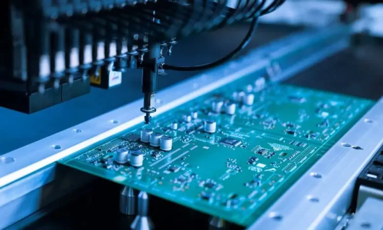
5. High-Precision SMT Assembly for Dense BGA and Fine-Pitch Designs
High-density assemblies demand advanced SMT capability. FastTurn PCB supports:
- 0.3 mm and smaller fine-pitch ICs
- Micro-BGA and CSP packages
- 01005 and 0201 passives
- Via-in-pad BGA escape routing
- 2D & 3D solder paste inspection (SPI)
- X-ray analysis for hidden-joint components
SMT reliability is especially critical for HDI assemblies, where solder joint defects can compromise signal routing beneath BGA packages.
6. Thermal Management Engineering for High-Power Multi-Layer Boards
Multi-layer PCBs often suffer from heat accumulation, especially in EV electronics, power modules, and IoT devices.
FastTurn optimizes thermal reliability through:
- Thick-copper structures
- Thermal via arrays
- Copper coin and heat dissipation features
- Balanced thermal distribution in stackup design
- Controlled reflow temperature profiling
This ensures stable performance even under continuous or high-load operation.
7. Full Turnkey Workflow Ensures Reliability Across All Stages
One of the biggest reasons OEMs choose FastTurn PCB is its fully integrated turnkey workflow, which eliminates the inconsistencies that occur when fabrication, sourcing, and assembly are separated.
Turnkey workflow includes:
- PCB fabrication
- Component sourcing
- SMT/THT assembly
- AOI, X-ray, and functional testing
- Final packaging and logistics
This is especially important for HDI and multilayer boards, where misalignment between fabrication and assembly can lead to:
Warpage
- BGA solder failures
- Impedance mismatches
- Thermal stress defects
By keeping the entire workflow under one system, FastTurn ensures consistent quality and predictable reliability.
8. Comprehensive Testing for High-Reliability Applications
FastTurn PCB performs a wide range of tests to ensure HDI and multilayer PCB performance:
- AOI inspection for all SMT placements
- X-ray inspection for BGA, QFN, and via-in-pad structures
- Functional testing (per customer requirements)
- High-voltage insulation testing
- Thermal cycling and reliability validation
- Microsection analysis for multilayer integrity
This makes FastTurn a preferred partner for OEMs building mission-critical electronics.
9. Why OEMs Trust FastTurn PCB for Complex, High-Density Turnkey Assembly
Global OEMs rely on FastTurn PCB because it offers:
- High-precision fabrication
- Reliable HDI processes
- Strong via and solder joint reliability
- Engineering-driven stackup and material selection
- Excellent SMT capability
- Full turnkey integration
- Transparent communication and QC documentation
In industries where reliability cannot be compromised, FastTurn stands out as a dependable manufacturing partner.
Conclusion
Multi-layer and HDI PCB assemblies represent the backbone of modern electronic innovation—but they also pose significant challenges in manufacturing reliability, electrical performance, and process consistency.
ensures high reliability across all multilayer and HDI builds through:
- Advanced lamination control
- High-precision drilling and microvia formation
- Controlled impedance engineering
- Material and surface finish optimization
- High-precision SMT processes
- Full turnkey workflow integration
- Comprehensive testing and documentation
For OEMs seeking guaranteed reliability, FastTurn PCB offers the engineering depth, manufacturing precision, and supply-chain stability essential for next-generation electronics.


